Key Components of a Flex PCB Board
omponents of a Flex PCB Board
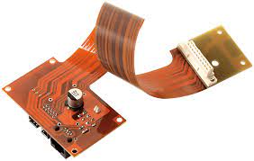
The key components of a flex PCB board include the base substrate, copper foil, dielectric coverlay and conductive paths. Flex PCBs are used to connect and power a wide variety of devices from wearable fitness trackers that monitor heart rate and calories burned, to high-tech drones and automobile dashboard systems that use dozens of sensors and microprocessors to perform everything from climate control to GPS navigation. They can be made in a range of sizes and shapes that integrate form, fit and function into the final product.
Unlike rigid PCBs, flex circuits are built on a flexible base substrate that can withstand bending and stretching without damaging the copper layer or the conductors. The most common flex substrate is polyimide, also known as Kapton. It is processed through lamination and curing to provide the mechanical strength and flexibility needed by a flex circuit. Other flex substrate materials are polyester (PET) and glass fiber-based epoxy. In a multi-layered flex pcb board, the base substrate is called a flexible copper-clad laminate (FCCL).
The core component of an FCCL is a patterned layer of ultrathin rolled annealed copper foil. The patterned copper layer is laminated to a dielectric or insulator. The most common insulator is polyimide film, but a variety of other films including PET, epoxy and glass fiber can be used. In addition to insulating the copper, the film can also insulate the conductive traces from corrosion and damage.
Key Components of a Flex PCB Board
These insulating films are typically coated with a solderable surface finish. Typical finishes include electroless nickel with silver, gold and organic palladium immersion gold. These coatings prevent the copper from oxidizing, make it easier to solder, and protect it from environmental damage.
While flex circuits offer many advantages over rigid PCBs, they are not without limitations. These challenges can be overcome with good design and manufacturing practices.
For example, a flex circuit should be designed with the maximum number of conductors possible within a given area. The layout should also be engineered to limit stress points in the flex area, such as vias and slits. Conductors should be routed perpendicular to the bend radius, rather than zigzagging around it. This will minimize stress points that can cause traces to break, as well as improve impedance and control in the flex area.
In addition, the conductive paths should be carefully spaced. Stacking conductive paths near each other creates points of stress that can lead to failure and reduce the overall life of the circuit. Conductors should also be oriented to the expected flexing direction to avoid damage or shorting during assembly and use. Finally, the edges of the traces should be rounded to increase tear resistance and improve aesthetics. PCBWay’s detailed calculator is a great tool to help you optimize your design. It can show you how much your flex PCB will cost and how it can be improved. To get started, click here.